
红外探测器是国防安全、环境监测、医疗诊断、工业检测以及自动驾驶和智能感知等领域的重要基础器件。随着应用场景向高复杂度、低功耗和自主化方向发展,下一代红外系统需要同时具备高探测率、快速响应、多维信息获取、紧凑集成和片上智能处理能力。传统HgCdTe、InSb、InGaAs、量子阱等材料体系仍具有高性能优势,但在制冷需求、暗电流控制、制备成本和功能拓展方面仍面临限制。
近日,复旦大学智慧纳米机器人与纳米系统国际研究院/智能机器人与先进制造创新学院梅永丰教授团队联合中国科学院上海技术物理研究所吴斌民博士、甄红楼研究员等,在材料领域一区Top期刊Advanced Materials发表综述论文《Recent Progress in Infrared Detection From Material Advances to Integrated Intelligent Systems》。该文围绕“材料-器件-系统”三个层级,系统梳理了红外探测从高性能探测单元向集成化、智能化、多功能平台演进的最新进展。
在材料层面,本综述总结了传统红外材料通过能带调控、异质结设计、势垒结构和低暗电流工程提升器件性能的研究进展,并重点讨论了HgCdTe、量子阱、II型超晶格和量子点等体系在高工作温度探测、低噪声探测和多波段响应方面的代表性突破。同时,新兴的二维材料、黑磷、过渡金属硫族化物、纳米薄膜和热敏材料等新材料体系为室温宽谱、偏振敏感、柔性化及片上集成红外探测提供了新的材料基础(见图1)。
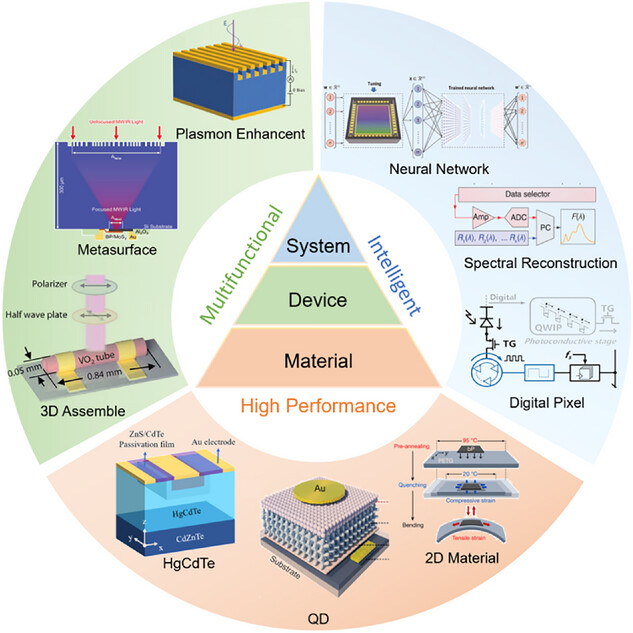
图1:红外探测技术在材料、器件与系统层面的研究进展框架
在器件层面,本综述进一步讨论了等离激元、超表面和三维自组装纳米薄膜等微纳结构对光场耦合、选择性吸收、偏振响应和入射方向识别的调控作用。通过增强光-物质相互作用、延长有效光程并引入可设计的曲面或三维微纳结构,红外探测器可突破传统平面器件功能单一的限制,实现波长、偏振、角度等多维信息融合探测。综述进一步从光子探测、热探测以及光热电探测等基本机制出发,对响应率、比探测率、时间响应和暗电流来源进行了系统归纳,为器件性能优化建立了清晰的物理框架。
在系统层面,本综述总结了微型光谱仪、传感内计算、神经形态架构和数字像素焦平面阵列等片上集成方案。相关技术可将红外感知、存储、计算和信号处理集成在单芯片平台中,实现自适应感知、数据压缩、实时重构和智能识别。该综述从材料创新、微结构设计到系统架构三个尺度建立了较完整的红外探测发展图谱,为紧凑型智能红外系统、多功能成像、分布式传感、健康监测和片上光计算等应用提供了重要参考。
复旦大学智慧纳米机器人与纳米系统国际研究院/智能机器人与先进制造创新学院章城、牛艺霖和张子煜为该论文共同第一作者;中国科学院上海技术物理研究所吴斌民博士、甄红楼研究员和复旦大学梅永丰教授为该论文共同通讯作者。该工作得到了国家自然科学基金、中国科学院战略性先导科技专项、上海市科委、中国博士后科学基金及上海市超级博士后等项目的资助和支持。
文章信息:
Cheng Zhang#, Yilin Niu#, Ziyu Zhang#, Binmin Wu*, Honglou Zhen*, Gaoshan Huang & Yongfeng Mei*, Recent Progress in Infrared Detection From Material Advances to Integrated Intelligent Systems, Advanced Materials, 2026, 38, e21432.
原文链接:https://doi.org/10.1002/adma.202521432
Recent Progress in Infrared Detection From Material Advances to Integrated Intelligent Systems
Growing industrial, environmental, and healthcare needs are accelerating the development of next-generation infrared systems with high detectivity, multifunctional sensing, and on-device intelligence. While traditional devices (e.g., HgCdTe, quantum wells) continue to dominate in terms of performance, they face limitations in cooling requirements, cost, and functionality. Recently, considerable advances have been made in materials, structures, and detection systems. As the foundation of IR systems, photodetectors based on traditional materials with band alignment engineering and emerging materials (e.g., two-dimensional materials and quantum dots) show high photodetectivity, low dark current, and room-temperature operation. Meanwhile, on-chip microstructures (e.g., plasmons, metasurfaces, and 3D-assembled architectures) integration enables manipulation of coupling and propagation of electromagnetic fields, which enhances polarization and wavelength-dependent light absorption. These developments empower infrared devices with multidimensional photodetection capabilities and tunable spectral response. Furthermore, advanced technologies like in-sensor computing, miniaturized spectrometers, and on-chip digitization merge sensing, storage, and computing into a single chip. The integration enables monolithic infrared systems with more compact architectures while possessing adaptive perception, data compression, and real-time signal processing capabilities. Finally, a comparative analysis containing material engineering, microstructure design, and integrated architecture is presented to outline the challenges and opportunities toward compact, intelligent, multifunctional infrared detection platforms.
审核:黄高山、陈相仲