薄膜自卷曲技术是一种将平面薄膜自发转化为三维管状结构的微纳制造方法。相较于传统平面器件,这种由二维到三维的构筑方式有望显著降低器件占地面积,提升空间利用率,并为电、光、磁等多物理场耦合提供新的结构设计自由度。在传统平面集成逐渐受到尺寸、功耗和热管理限制的背景下,薄膜自卷曲技术为高密度、微型化和多功能片上系统提供了一条具有潜力的实现路径。
近日,我院崔继斋副教授课题组受邀在《Materials Today Electronics》发表题为《Recent advances in rolled-up on-chip devices》的综述论文,系统总结了薄膜自卷曲片上器件的研究进展,并对其关键制备策略、典型器件体系以及未来发展方向进行了归纳与展望。
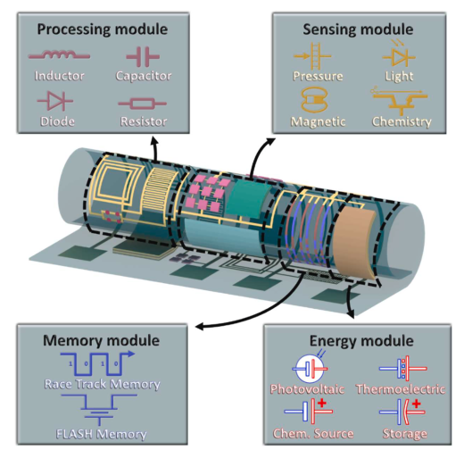
图1. 基于薄膜自卷曲技术的片上电子系统
该综述围绕薄膜自卷曲片上器件的发展脉络展开,重点梳理了卷曲结构的形成机制与加工方法,并总结了该技术在无源器件、传感器件、信息存储与处理器件以及微型能源器件等方向的代表性进展。文章认为,薄膜自卷曲技术兼具平面工艺兼容性与三维结构优势,在推动片上器件向更高集成度、更小尺寸和更多功能演进方面具有重要研究价值。同时,文章也指出,欧姆损耗、热积累以及封装可靠性仍是该领域进一步走向应用需要解决的关键问题。总体而言,该工作系统展示了薄膜自卷曲技术从基础机理、结构构筑到器件实现的发展现状,为三维片上电子器件的后续研究与应用提供了重要参考。
本论文第一作者为复旦大学智慧纳米机器人与纳米系统国际研究院博士生陈力、迟宇航、刘声宝,崔继斋副教授为论文的通讯作者。该工作得到了国家重点研发计划、国家自然科学基金、上海市科委等项目的资助和支持。
文章信息:Li Chen, Yuhang Chi, Shengbao Liu, Gaoshan Huang, Yongfeng Mei, Jizhai Cui*. Recent advances in rolled-up on-chip devices. Materials Today Electronics, 2026, 16: 100213.
文章链接:/_temp/f6813b45-fbd9-49f0-bbf2-2736905d09e6.pdf
Recent Advances in Rolled-up On-Chip Devices
Thin-film rolled-up technology is a micro-/nanofabrication strategy that enables the spontaneous transformation of planar thin-film structures into three-dimensional tubular architectures through the release of built-in strain. Compared with conventional planar devices, it can markedly reduce the device footprint, improve spatial utilization, and introduce new opportunities for multiphysics coupling among electrical, optical, and magnetic functionalities. As emphasized in this review, as conventional planar integration is increasingly limited by device scaling, power consumption, and thermal management, thin-film rolled-up technology represents a promising route toward high-density, miniaturized, and multifunctional on-chip systems.